
Design for Manufacture
Products that can be manufactured more easily are cheaper to produce and generally higher quality too.
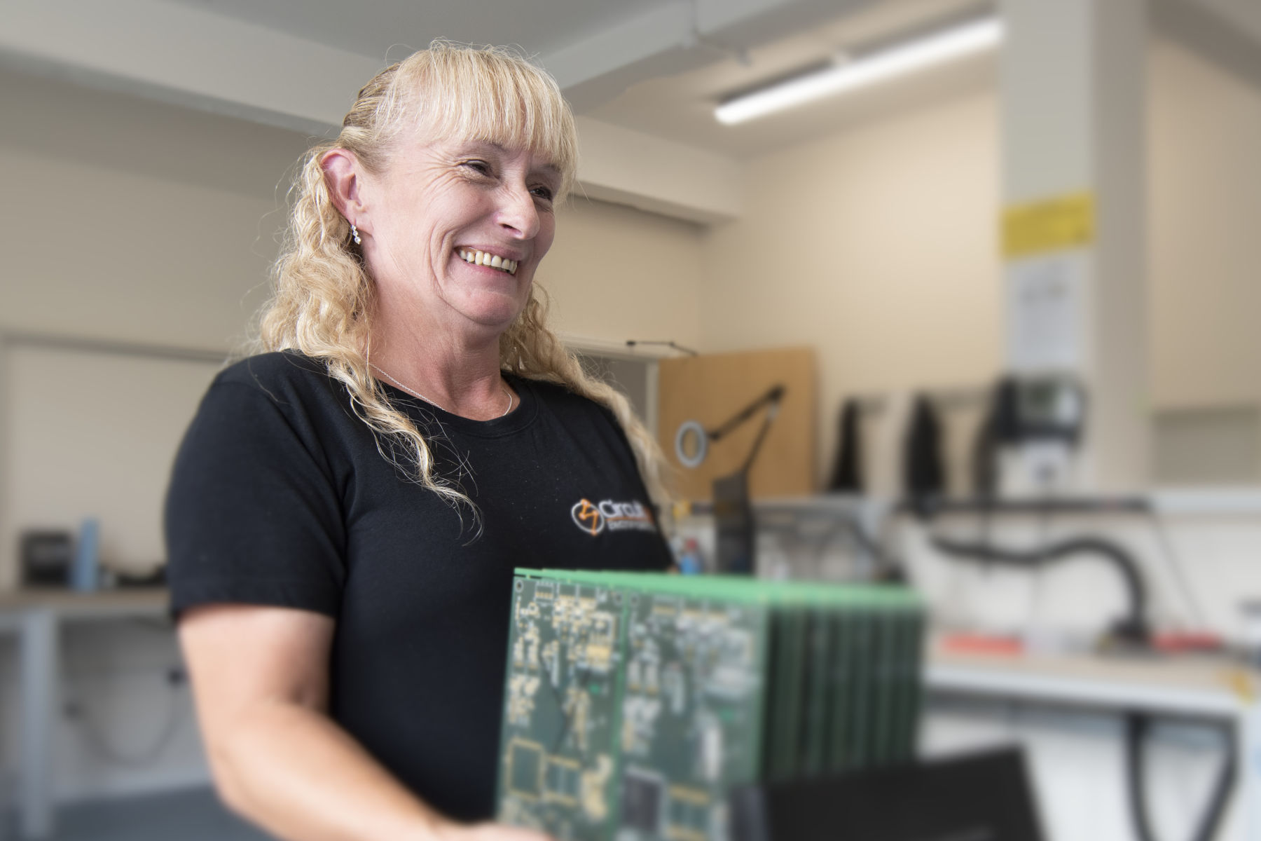
Our engineers take manufacturability into consideration throughout the design process.
PCB Design for Manufacture
When we design our PCBs, we consider two aspects of DFM: design for fabrication and design for assembly.
Fabrication is the complex process of making the actual boards themselves, with many steps including creating film images, printing and etching the copper tracks and pads, stacking and bonding multiple layers together, drilling very precise holes for vias and components, electroplating, applying solder mask, surface finishing and silkscreen (legend) printing.
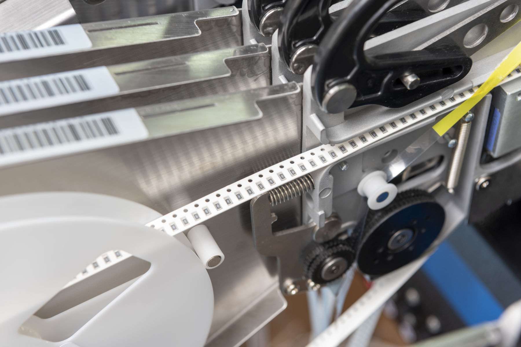
PCB assembly is the process of positioning components on the circuit board and connecting them both electrically and mechanically, which is the part of PCB manufacturing we do in-house (hand-soldering or automated pick and place).
Our engineers have a solid understanding of both PCB fabrication and PCB assembly, meaning our circuit boards are designed for manufacture right from the outset.
Manufacturing Documentation
Detailed, unambiguous and comprehensive documentation is key to ensuring your PCB is built exactly as intended.
When releasing a design for manufacture, our engineers generate a comprehensive pack of manufacturing documentation including extended gerber files (which specify the layout of the different layers of the PCB, such as the copper, soldermask, silkscreen / legend and solder paste layers), drill files, XY data to denote exact component placement, PCB specification and a full Bill of Materials (BoM), ready for the PCB fab's data analysis and production tool generation steps.
Technical Considerations
Manufacturability issues can also arise at the data generation stage during PCB layout.
Tombstoning, hot spots, cold spots, solder escape, copper balancing, drill hole aspect ratio, annular ring size, fiducials, clarity of silkscreen (legend), alignment, spacing, edge clearance, pad size, footprints, track widths, via positions, overhanging components and panelization are just some of the aspects of PCB manufacturability our engineers take into consideration when designing your printed circuit board!
Quality Processes
From design guidelines, checklists, and peer reviews through to automated Design Rule Checks and close working relationships with PCB fabs, our ISO 9001 quality processes ensure your boards are well designed and ready for manufacture.
And as we assemble PCBs as well as design them, you can be sure our engineers will lay out boards that can actually be manufactured effectively too!
Instant feedback and continuous communication between our production technicians and design engineers allows us to evaluate and improve board designs throughout the prototyping stages, ready for pre-production and volume manufacture.